Full Text:
Since the discovery of the remarkable properties of graphene, scientists have increasingly focused research on the many other 2-D materials possible, both those found in nature and those concocted in the lab. However, growing high-quality, crystalline 2-D materials at scale has proven a significant challenge.
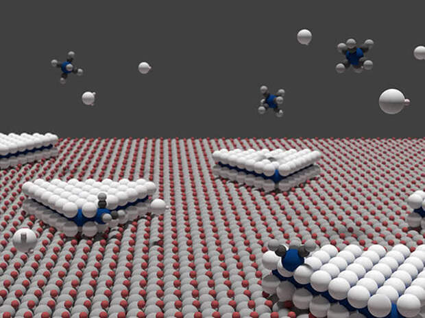
A pair of papers published online in two nanotechnology journals recently provide the basis for growing wafer-scale 2-D crystals for future electronic devices. Researchers have developed a multistep process to make single crystal, atomically thin films of tungsten diselenide across large-area sapphire substrates. The process uses sapphire as the substrate because of its crystalline structure. This structure orients the film growth in a crystal pattern in a process called epitaxy. As small islands of the material form on the substrate and the substrate is heated, the islands spread out across the substrate in a uniform pattern, forming a large-area film without gaps and with very few defects. The key advance was the use of gas-source chemical vapor deposition to precisely control the island density and rate of spreading to achieve a single layer of the 2-D material.Image credit: Xiaotian Zhang/Penn State
